Atomic Force Microscope (AFM) and Scanning Tunneling Microscope (STM)
Our setup:
Our microscope is a modular MultiMode AFM/STM (Bruker/Digital Instruments, Santa Barbara, CA) equipped with a Nanoscope VI controller. By exchanging the scanner a wide scan range in the xy plane is accessible ranging from atomic resolution to more than 100 µm. In z direction the scan range is limited to 3 µm. The modular architecture of the microscope facilitates a 3D mapping of various surface properties beside topography as for instance phase shift or friction. Both, STM and AFM are able to image either at ambient conditions or in liquid at controlled electrochemical potentials for sample and tip.
Atomic force microscopy
The atomic force microscope (AFM), or scanning force microscope (SFM) was invented in 1986 by Binnig, Quate and Gerber. Like all other scanning probe microscopes, the AFM utilizes a sharp probe moving over the surface of a sample in a raster scan. In the case of the AFM, the probe is an ultra sharp tip attached to a cantilever, which bends in response to the force between tip and sample.
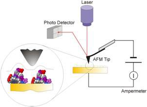
Figure 1 illustrates the working principle of an AFM: as the cantilever flexes, the light from the laser is reflected onto a photo-diode. Since the cantilever obeys Hooke's Law for small displacements, the interaction force between the tip and the sample can be determined. The actual forces between the tip and the sample surface are extremely small, usually less than 10-9 N. Therefore, hard materials like solid as well as soft matter like proteins can be scanned. The movement of the tip or sample is performed by a highly precise positioning device made from piezo-electric ceramics, most often in the form of a tube scanner. The scanner is capable of performing sub-angstrom displacements in x-, y- and z-directions. The z-axis is conventionally perpendicular to the sample. The images can be acquired in different ways which rely on different types of interaction between tip and surface. The three main classes of imaging modes are contact mode, tapping mode and non-contact mode. Tapping mode is in our days the most common mode used in AFM. When operated in air or other gases, the cantilever is oscillated at its resonant frequency (often hundreds of kilohertz) and positioned above the surface so that it only taps the surface for a very small fraction of its oscillation period.
STM
Scanning tunneling microscopy (STM) measures topography of a sample surface by applying a small bias between the sample and an atomically sharp tip and measuring the resulting tunneling current as feedback information. Both, sample and tip have to be conducting or semiconducting. The measured current between tip and surface depends exponentially on the distance between them. STM is able to reveal the electronic structure of the sample surface and facilitates the investigation of the electronic structure of molecules.
Contact:
Elke Brauweiler-Reuters
Tel.: +49-2461-61-5411
e-mail: e.brauweiler-reuters@fz-juelich.de
Dr. Dirk Mayer
Tel.: +49-2461-61-4023
e-mail: dirk.mayer@fz-juelich.de