Vision
New technologies and materials for the future
Technological progress is closely linked to the materials and processes at our disposal. In our research group, we use a shadow mask technology we have patentedand topological insulators to solve problems in the research fields of topological and conventional quantum computing. A quantum computer is a processor that performs computations based on quantum states and could solve specific computational tasks faster than conventional computers. These specific computational tasks include encryption and optimization tasks.
The challenges in the field of quantum computing are manifold, so that many questions can only be solved in cooperation with scientists from several disciplines. Therefore, we collaborate with many partners from Germany and abroad in several projects. Within our group we work on the aspects of simulation of quantum systems, fabrication of quantum chips as well as their characterization.
Topological insulators - a new class of materials
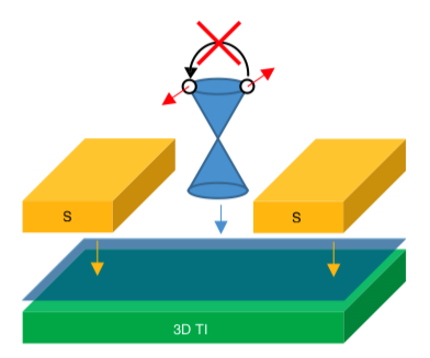
Topological insulators are a relatively new class of materials whose existence was first experimentally demonstrated in 2007. Topological insulators are solids that can enter a so-called topogical phase, in which the interior of the solid behaves like an electrical insulator, while the surface conducts electricity with almost no losses1. Due to the low (thermal) losses, topological insulators are interesting for the semiconductor industry. Another possible application is topological superconducting qubits, where a topological insulator is combined with a superconductor. The global topological phase could be resistant to local noise and thus overcome the problem of limited coherence time in today's qubits.
Topological insulators are a relatively new class of materials whose existence was first experimentally demonstrated in 2007. Topological insulators are solids that can enter a so-called topogical phase, in which the interior of the solid behaves like an electrical insulator, while the surface conducts electricity with almost no losses1. Due to the low (thermal) losses, topological insulators are interesting for the semiconductor industry. Another possible application is topological superconducting qubits, where a topological insulator is combined with a superconductor. The global topological phase could be resistant to local noise and thus overcome the problem of limited coherence time in today's qubits.
Shadow technology
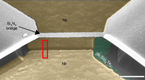
Thin film technology is a central technology in semiconductor electronics and is used, among other things, to fabricate integrated circuits. To combine selective growth of topological insulators with established fabrication methods thin film technology we have developed a new shadow mask technology described in Schüffelgen et aI. Here, we use silicon dioxide and silicon nitride with layer thicknesses to create a mask for selective growth of topological insulators. A second thicker layer of silicon dioxide and silicon nitride is used to create a shadow cast during the growth of superconducting materials. The resulting material systems are heterostructures of superconductors and topological insulators.
According to theoretical predictions, these material systems can be used to build topological quantum computers based on so-called Majorana-Zero modes (MZMs). The results presented in Schüffelgen et al are consistent with the theoretical expectations for a system using MZMs. The technology can also be scaled up.
From simulation to growth to application
The challenges in researching topological insulators and quantum computers are complex. Therefore, our team has a versatile setup. The different tasks for the development of new quantum chips can be divided into the three subareas of simulations, growth and measurements. These areas are by no means completely independent of each other but intertwine.
Simulations
Simulations and modeling of nanostructures play an important role in the design and evaluation of quantum chips and experiments. Through modeling, both the device geometry and the material composition of quantum chips can be adapted to the respective experiment. In addition, simulations enable an evaluation of the often complex data from experiments. In particular, in the project "Building Blocks for Quantum Computing based on Topological Materials with Experimental and Theoretical Approaches", one focus of our group is on simulations.
Growth
Topological insulators are grown in ultra-high vacuum chambers in molecular beam epitaxy facilities. The quality of the topological insulators strongly depends on the growth parameters such as material flow, substrate temperature and surface cleanliness of the substrate. By choosing the growth parameters in combination with the shadow mask, we can also achieve selective growth of the topological insulator in lithographically defined areas of the substrate.
The molecular beam epitaxy facilities are part of the Jülich nanocluster. This gives us access to other classes of materials and allows us to combine the topological insulators with superconductors, among others, to form heterostructures. In addition, we use the Helmholtz Nanofacility to prepare our substrates and postfabricate the quantum chips after growth.
Measurements

After completion of a quantum chip, it is usually measured at millikelvin temperatures, since the quantum phenomena we want to observe can only be observed at low temperatures. These measurements are performed in our cryostat lab, Lab 13. It contains two mixed cryostats, each equipped with strong vector magnets with which we can apply magnetic field strengths in the tesla range.
The cryostats are optimized for different experiments. One cryostat is optimized for low-noise low-frequency transport measurements with magnetic fields up to 6 Tesla. The second cryostat is optimized for both low-frequency transort measurements and high-frequency measurement of superconducting qubits.
High quality materials
We are also optimizing the shadow mask technology independently from the growth of topological materials. The advantages of the mask over polymer-based masks is that 1) thorough cleaning of all surfaces prior to material growth is possible 2) the mask can be used in ultra-high vacuum chambers and 3) the mask is temperature stable. For these reasons, we are exploring the use of the mask for conventional superconducting qubits to increase coherence times as well as for novel growth methods, as in the TLE4HSQ project.
1 This description applies to so-called 3-dimensional topological insulators. In 2-dimensional topological insulators, the surface is insulating and the outer edges are electrically conductive.