Spectroscopy
The challenging era of scientific research and industrial developments in the ongoing 21st century will be predominantly driven by the strong need for observing, understanding, developing and improving novel materials, devices and technologies, making them more efficient with respect to their function and their energy and resources consumption. To this end, new insights into applied physics, chemistry and biology are needed and correlative spectroscopy is extremely important.
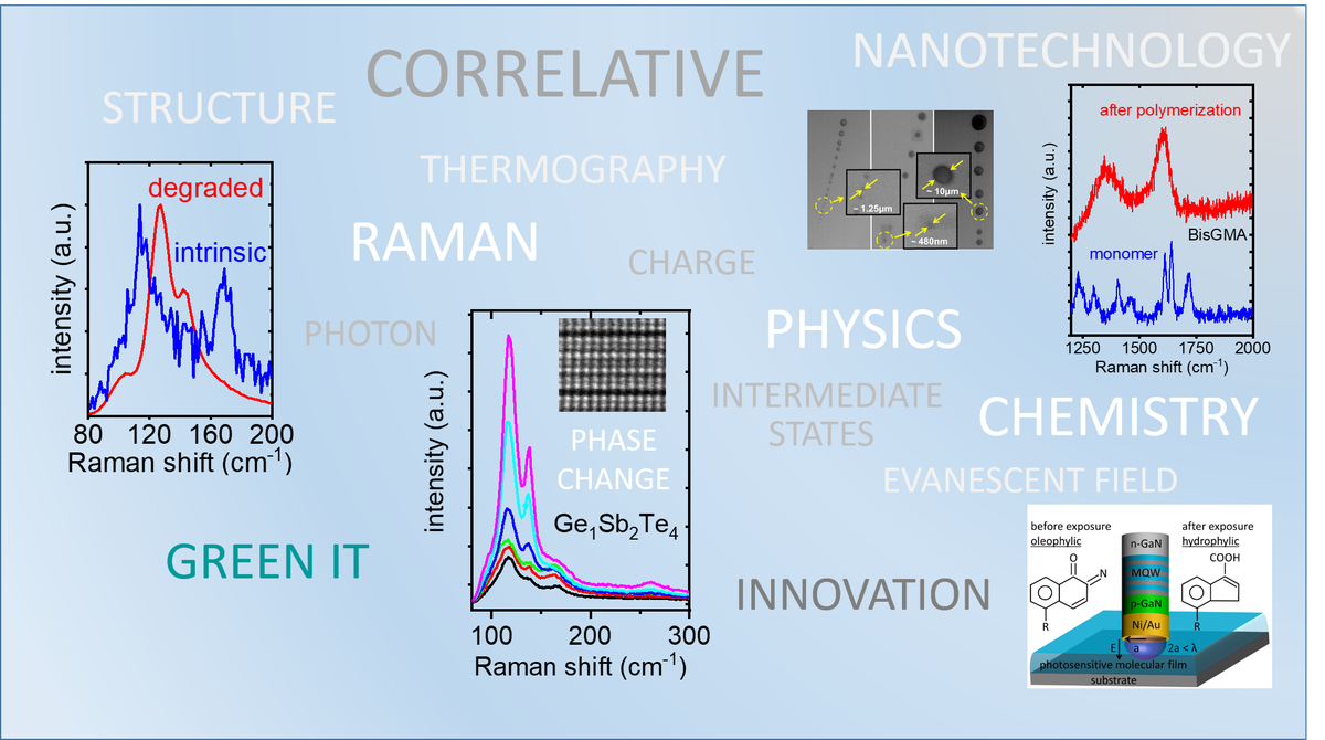
On the one hand, we employ Raman spectroscopy as a powerful, non-destructive characterization tool associated with the scattering of light by optical phonons in solids and molecular vibrations. Here, monochromatic light, typically a laser, scatters and interacts with materials. The oscillating electromagnetic field of photons induces a polarization of the molecular cloud and generates vibrational excited states (rotational and other low frequency energy modes may also be found).
These short-lived states are not stable and scattered photons are emitted. The energy of the vibration transition is related to the vibration frequency. The spectra therefore contain chemical and structural information. This method is not only used to investigate chemical bonding, composition and free carrier concentration in the compounds but also to determine the strain and the temperature in the materials and devices under investigation.
On the other hand we employ photoluminescence spectroscopy for semiconductors. Photons with an energy higher than the band gap are absorbed and carriers are excited inducing the formation of electron-hole pairs. The carriers undergo non-radiative relaxation processes before radiative recombination is observed. This method is used to determine the band gap, to investigate non-radiative recombination centers such as defects and to study the optoelectronic properties in semiconductor nanostructures and devices.
Both methods are employed to correlate the optoelectronic material properties to their structure down to the atomic level as well as to their functional and device characteristics.
Examples:
Laser micro annealing, effect on degradation and charge transport in nanostructures
Curing of processing damage and correlation to efficiency, reliability and yield
Observation of chemical reactions for structuring processes
Utilization of phase change and intermediate states in transmistor devices
Contact:
