Memristive devices
Non-volatile memories can retain stored information even after their power is removed. They play an important role in future information technology and give rise to novel concepts for neuromorphic computing. A promising type of non-volatile memories is based on resistive switching, which is found in two different groups of materials with distinct switching mechanisms. One group of materials is Ge-Sb-Te based chalcogenides where the resistive switching mechanism is based on the reversible phase-change between the amorphous and the crystalline state.
The other group of materials is metal oxides in which resistive switching is achieved through a reversible redox-based valence-change between the high and the low valence state of the metal. Devices comprising a metal-insulator-metal (MIM) structure, where the insulator can be a phase-change material (PCM) or a valence change material (VCM), are called memristors. They show hysteresis I-V curves, where the different slopes of the curves represent different values in the resistance allowing to encode the binary information ‘1’ and ‘0’.
Owing to an increasing demand for the miniaturization of the devices, it is therefore of both fundamental and technological importance to characterize the phase-change and valence change at the atomic scale.
We strive to develop techniques for quantitative transmission electron microscopy (TEM), data analysis, and modeling of TEM experiments and materials, and to apply these techniques to the characterization of surfaces, interfaces, and defects in memristive materials and devices. The developed TEM techniques enable us to correlate the observed individual atoms to local material properties, thereby making it possible to establish the structure-property relationship down to the atomic level.
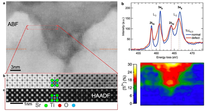
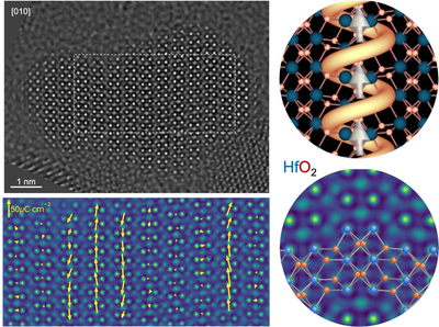
We have, for example, applied monochromated electron energy loss spectroscopy (EELS) in aberration-corrected scanning TEM (STEM) to quantitatively map the 4+ to 3+ Ti valence changes in nanoscale conducting filaments in a memristor based on an Fe doped SrTiO3 thin film [1]. For another remarkable example, we used the negative spherical aberration imaging (NCSI)technique in aberration-corrected conventional TEM (CTEM) and revealed the origin of the nanoscale ferroelectric phase at twin boundaries in twinned HfO2 nanocrystals by precisely resolving both the heavy Hf and the light O atoms [2].
Literature:
[1] H. Du, C.-L. Jia, A. Koehl, J. Barthel, R. Dittmann, R. Waser, J. Mayer, Chem. Mater. 29 (2017) 3164–3173 (doi: 10.1021/acs.chemmater.7b00220).
[2] H. Du, C. Groh, C.-L. Jia, T. Ohlerth, R.E. Dunin-Borkowski, U. Simon, J. Mayer, Matter. 4 (2021) 986–1000 (doi: 10.1016/j.matt.2020.12.008).
[3] H. Du, C.-L. Jia, L. Houben, V. Metlenko, R.A. De Souza, R. Waser, J. Mayer, Acta Mater. 89 (2015) 344–351 (doi: 10.1016/j.actamat.2015.02.016).
[4] H. Du, C.-L. Jia, J. Mayer, J. Barthel, C. Lenser, R. Dittmann, Adv. Funct. Mater. 25 (2015) 6369–6373 (doi: 10.1002/adfm.201500852).
[5] H. Du, C.-L. Jia, J. Mayer, Faraday Discuss. 213 (2019) 245–258 (doi: 10.1039/C8FD00102B).
Contact:
