Nano-Spintronics-Cluster-Tool
The Nano-Spintronics-Cluster-Tool is a dedicated experimental platform for magnetism- and spintronics-related activities in our institute and integrates various complementary methods into a single instrument within an ultrahigh vacuum environment (UHV).
A central part of the Nano-Spintronics-Cluster-Tool is a high-resolution scanning electron microscope (SEM). The spatial resolution limit at high beam energies (30 keV) is 3 nm, while a beam booster improves the resolution at low beam energies (down to 0.1 keV). A high beam current of up to 5 nA in combination with an electron spin polarization detector allows fast structural and magnetic studies (SEMPA) to be carried out on the mesoscale at variable temperatures (700 down to 30 K).
The magnetic nanoscale is accessed by means of an integrated low-temperature spin-polarized scanning tunneling microscope (SP-STM) operating at temperatures as low as 4.5 K. The sample preparation chamber features a variety of proven surface science techniques. Ultra-thin films can be deposited from nine electron-beam evaporation sources. A dedicated chamber allows magnetic molecules to be deposited by various methods.
Reflection high-energy electron diffraction (RHEED) during evaporation and low energy electron diffraction (LEED) together with scanning tunneling microscopy (STM) allow atomic scale structural characterization. Chemical composition and the cleanness of surfaces are determined with Auger electron spectroscopy (AES) and x-ray photoemission spectroscopy (XPS). Magneto-optical Kerr effect (MOKE) measurements permit in-situ magnetic characterization of magnetic thin film systems.
Finally, the system provides three approaches for in-situ structuring: (i) shadow deposition through microapertures for contact pads, (ii) focused ion beam (FIB) etching in dual-beam configuration with the SEM for writing arbitrarily-shaped structures of sizes down to 20 nm, and (iii) scanning tip structuring by STM for length scales below 20 nm. Thus, 6 orders of magnitude in sample size can be covered. The STM and SEM stages feature four electric contacts to the sample, which allow in-situ electric transport measurements.
Dr. Frank Matthes
Dr. Daniel E. Bürgler

Figure: Top view of the Nano-Spintronics-Cluster-Tool: The left chamber houses the SEM, the spin polarization detector, and the FIB. The chamber on the right side contains the low temperature STM in the front part with the preparation and analysis chamber at the back. A transfer chamber (middle) connects the two units and enables in-situ access to all attached preparation and characterization tools without a vacuum break.
Magnetic contrast with SP-STM
We tested the performance of the STM and the ability to achieve spin contrast by investigating thin (1–2 ML) Fe films on W(110), the standard test system for SP-STM [O. Pietzsch et al., Phys. Rev. Lett. 84, 5212 (2000)]. An in-situ grown Fe wedge is studied in an area, where the Fe film is 1.5 ML thick and thus exhibits areas with one or two ML Fe coverage, respectively. We used a wet chemically etched tip made of antiferromagnetic bulk Cr. The figure shows the simultaneously acquired topography (a) and differential conductivity (dI/dV) map at E-EF=-300 meV (b) as well as a 3D representation of the topography colored according to the spectroscopic data (c). The experiment was performed at 4.8 K.
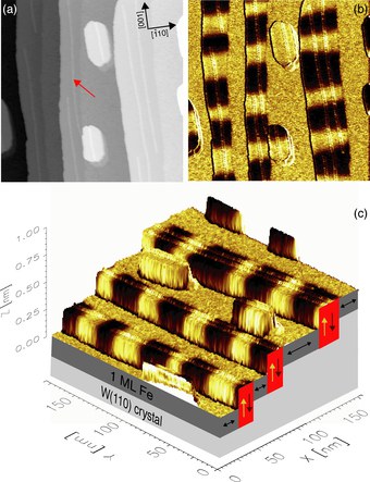
The topography image (a) was measured in the constant-current mode with a gap voltage of -300 mV addressing occupied states and a tunneling current of 2.5 nA. The scan area (180 nm x 180 nm) comprises 3 surface steps of the W(110) substrate and spans a total height difference of about 0.8 nm including the islands on the topmost terrace. The post-annealing treatment at 560 K causes the Fe atoms in the second ML to diffuse to the step edges, where 2 ML high Fe stripes are formed [red marks in (c)]. Dislocation lines in the 2 ML areas [red arrow in (a)] run along the [001] direction. The simultaneously recorded dI/dV map at E-EF=-300 meV in (b) displays strong contrast in the 2 ML areas only. The dislocation lines appear as bright lines running along [001]. The alternating brown/yellow contrast is due to magnetic domains of the out-of-plane magnetized 2 ML-thick Fe film. The first Fe ML on W(110) is in-plane magnetized and does not contribute to the magnetic contrast of this image. The conductivity map was measured by lock-in detection at a frequency of 2700 Hz and a peak-to-peak modulation amplitude of 42 mV. The overlay of topography and dI/dV map in (c) gives a visual impression of the subtle nanoscale structure-magnetism correlation.
Results
- Deposition of Chiral Heptahelicene Molecules on Ferromagnetic Co and Fe Thin-Film Substrates
- Cyclophane with eclipsed pyrene units enables construction of spin interfaces with chemical accuracy
- Epitaxial and contamination-free Co(0001) electrodes on insulating substrates for molecular spintronic devices
- Ultra-High Vacuum Deposition of Pyrene Molecules on Metal SurfacesMagnetic subunits within a single molecule–surface hybrid
- Magnetic subunits within a single molecule–surface hybrid
- Magnetic surface domain imaging of uncapped epitaxial FeRh(001) thin films across the temperature-induced metamagnetic transition
- Adsorption phenomena of cubane-type tetranuclear Ni(II) complexes with neutral, thioether-functionalized ligands on Au(111)
- Structural integrity of single bis(phthalocyaninato)-Neodymium(III) molecules on metal surfaces with different reactivitye
- Accessing 4f-states in single-molecule spintronics
- Observation and implications of magnetic domains in lateral spin valves
- Detection of pure spin currents in in-situ fabricated and measured lateral spinvalves