LT Nanoprobe
Electrical probing of nanostructures
A major challenge in the development of molecular and spintronic nanodevices is their interconnection with larger scale electrical circuits required to control and characterize their functional properties. Local electrical probing by multiple probes with the ultimate precision of scanning tunneling microscopy (STM) and analytical capabilities of scanning tunneling spectroscopy (STS) can significantly improve efficiency in analyzing individual nanodevice approaches without the need for full electrical integration that conventionally requires extended fabrication techniques.
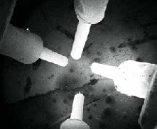
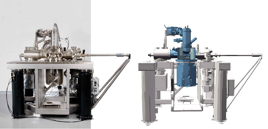
In order to meet the requirements for electrical probing of nanostructures Omicron has developed in collaboration with us the LT Nanoprobe, a sophisticated instrument specifically designed for local and non-destructive 4-probe measurements at low temperatures. Four fully functional STM scanners are located next to a sample stage on a support attached to a LHe cryostat. Efficient thermal shielding allows for temperatures well below 5 K, extremely low thermal drift, and thermal equilibrium of sample and probes. A high resolution, UHV-compatible scanning electron microscope (SEM) at sufficiently small working distance to the compact 4-probe STM is used to navigate the tips on the sample. The shared stack scanner allows coarse positioning of the sample within ±4 mm in both lateral directions at any temperature. The coarse positioning system of each probe enables the controlled displacement of the probes in a volume of 5 mm x 5 mm x 3 mm (XYZ). Each probe can individually be brought in tunnelling contact by means of an automatic approach. Alternatively, the probes can be manually approached until electrical contact is established. A TTL trigger-controlled switching technology specifically adapted to the pA-current regime is utilized to route signals to external measurement equipment. Thus, a structure of interest in the nanometre regime can be imaged by SEM and STM, selected, and contacted by the four probes under the guidance of the high resolution SEM for electrical measurements in tunnelling or ohmic contact regime.
Dr. Frank Matthes
Dr. Daniel E. Bürgler
STM performance
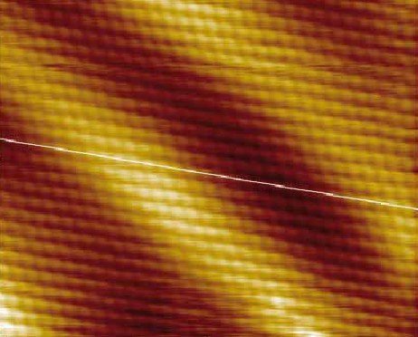
Each of the four scanner modules allows high-resolution and stable imaging as demonstrated by atomically resolving the Au(111) surface at 4.5 K. The constant-current mode STM data depicts the well-known Herring-bone superstructure superimposed with the hexagonal atomic lattice. The atomic corrugation is approximately 6 pm indicating a vertical stability of the LT Nanoprobe system in the low pm range. The image size is 21 nm x 25 nm (U = 310 mV, IT = 3 nA, raw data after slope subtraction).
Results
Direct measurement of anisotropic conductivity in a nanolaminated (Mn0.5Cr0.5)2GaC thin film